

The soldering guide for the USB Ultra IR receiver
Enough theory, lets go to the practice …
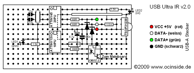
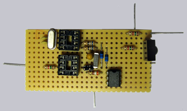
Here is a picture of the PCB layout with all construction units for easy soldering. Just watch it comfortably while your soldering iron (15-25 watt) is heating-up.
Here is the old USB Ultra IR v1.1 solder guide.
The correct position of the construction units …
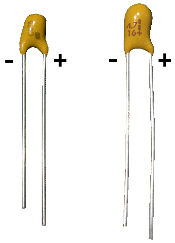
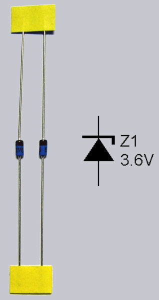
First we begin to plug in the construction units as explained on the 25 x 12 holes of the printed circuit board (PCB). Bent the pins under the PCB a little bit, but please DO NOT shorten the pins, yet !!! It is important that the small notches of the two IC sockets and the notch of the opto coupler with 6 pins are showing upward. The new Tiny45 IC got one small point instead of the notch to show the right direction. It is also necessary to pay attention to the polarity of both zener diodes (Z-diodes) and both Light Emitting Diodes, whereby the black ring of the Z-diodes have to show up to the direction of the IC notches. The polarity of LEDs is shown on a picture later on. Furthermore you must absolutely pai attention to the correct polarity of the small yellow 4.7 µF tantal capacitor, where the positive pin must show likewise upward like the IC notches! (beneath the 16 is a small plus (+) symbol to indicate the polarity of the construction unit). With the other construction units there is no polarity, so that only the correct position is important there.
Here again a picture with the different tantal capacitor designs and the polarity:
Here is a picture of the Z-Diodes / Zener Diodes polarity:
And here is a picture of the light emitting diodes polarity, whereby the shorter pin with the larger connecting surface and the reflector within the light emitting diode is the cathode/GND/ground/-/VSS. The longer pin with the smaller connecting surface within the light emitting diode is the anode/+/VCC:
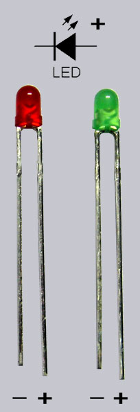
Once again a photo with the right positions whereby we place the LEDs later:
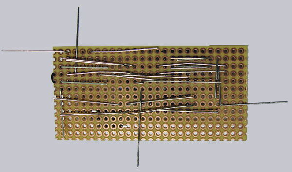
When all construction units except the LEDs are fixed attached, it continues with the lower surface. The 22pF capacitors of the quartz are not absolutely necessary but they are the load capacity for the quartz and should be soldered to a quartz. I’ve published another mirror-inverted picture so that one does not have to turn always the PCB for the detection of the right construction unit.
Here’s the mirror-inverted view ! for better orientation on the lower surface …
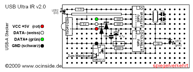
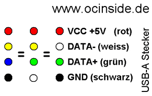
rot = red, weiss = white, grün = green, schwarz = black, Zum Mainboard = to the mainboard power switch spiegelverkehrt = mirrored
Correct bending and pinch off the pins …
On the basis of the photo one should bend now simply all pins of the construction units and pinch off the pins, whereby one again should make sure 100% that all construction units are on the correct position and as above explained also paid attention to the correct polarity. If you make an error in this step, it’s later rather difficult to out-iron – spend some time to bend all pins as shown and cut all pins in the correct length! with a long-nosed pliers and a small wire cutting pliers.
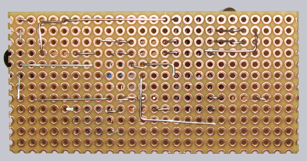
Thus the lower surface looks like after the bending all pins:
And in such a way looks the lower surface after cutting the pins:
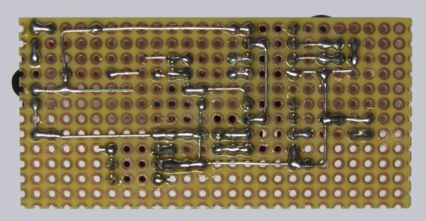
Now solder only the shown parts …
First we solder only all pins on the lower surface of the PCB as represented on the following Picture. Please do not solder everything, yet, but first times only each pin of the parts, since we still need the cables. Also absolutely consider here the free spaces, where no connection may be.
Now we solder still another small bridge (from one before cutted pin) to the right side. Simply bend one side approx. 2mm, put the wire, cut the correct length on the other side and then solder, so the bridge can not slip when soldering.
Now another solder bridge is added in the center of the two ICs. Here we can also use simply a piece from the material cutted before.
Solder the red low current LED and the green low current LED …
Now it is time for the two light emitting diodes, which must be polarized absolutely correctly, so that they can light up afterwards. The red LED is placed directly to the TSOP, whereby the shorter pin (-) points to the TSOP IR receiver. The green LED is put in near the Atmel ATTINY13V IC, whereby the longer pin (+) is soldered to the resistor and the shorter pin (-) to the small GND solder bridge, which we soldered on a while ago.
I consciously soldered the two LEDs now, because who ordered the new small IR receiver box from the Fanshop, of course would like to see the LEDs nevertheless. And this is only possible if the LED pins are left very long, so that the LEDs can be seen afterwards on the top side of the box. One should put the LED pins so far into the PCB, until the longer pin is seen approximately 8mm at the PCB bottom.
Who does not use the IR box, can solder both LEDs directly on the PCB. And who would like to place the PCB inside of a PC or HTPC, can use a 2-pol cable in order to attach the LEDs for example in a drive front bezel or in a Casesticker.
On the next picture you can see the four new soldered connections – two of the red LED in the left above the TSOP and two of the green LED right down near the lower IC socket.
Prepare the cables …
If you like to relax a little bit, it’s time to prepare the cables.
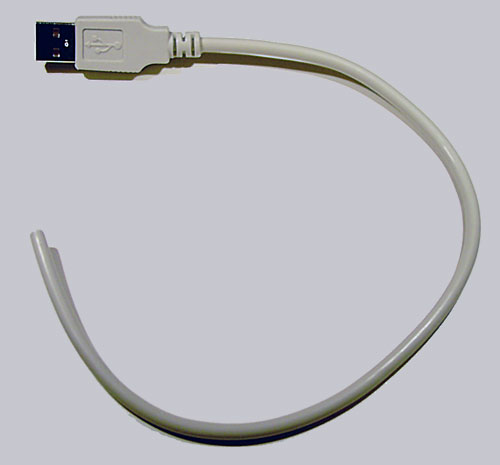
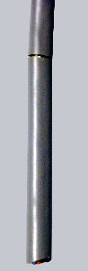
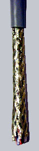
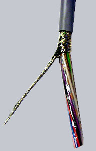
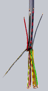
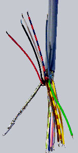
All cables are stripped approx. 3-4 cm, the outside shield is separated cleanly and then all individual wires have to be stripped and tin-plated. It makes sense to tin all wires to get the tin later easier and faster on the wires. Simply hold the soldering iron to the stripped wire and hold some tin to the other side solder. Repeat this with all wires.
Here is a small picture sequence how to strip it correctly …
Put the cables into the right PCB hole …
The small cable, which I could not unfortunately avoid in the layout, one can get oneself simply, cutting the USB cable or the 2-pole cable a few centimeter and taking one wire of it. Strip the wire approx. 2-3 mm, twine and tin-plate it as written before.
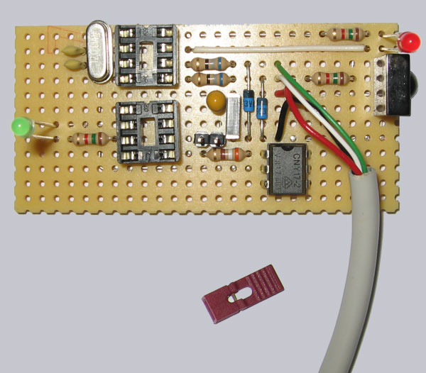
Now we put the cables with the explained colors in the correct place into the PCB.
The four wires of the USB cable are soldered this way: The red (VCC) cable is soldered to the middle TSOP pin, the 1.5 K resistor and the one side of the 100n capacitor. The black cable (GND) is soldered to the Jumper and the other side of the 100n capacitor. The white (or yellow) cable (DATA-) is soldered with the 68ohm resistor to pin 5 of the ATTiny45 IC and the green (or blue) cable (DATA+) is soldered with the other 68ohm resistor to pin 6 of the ATTiny45 IC.
Sometimes USB cables have different colors. Here is a table with some possible USB cable colors (just in case your cable is NOT red, black, white and green):
The last soldering act, where the remaining connections are soldered …
Now we solder as explained the remaining solder joints, whereby we must absolutely pay attention to all free spaces (e.g. the two pins of the tantal capacitor may not soldered together). If you still like to solder a little bit, you’re free to solder the GND shield of the USB cable with a short wire to a GND solder point of the circuit, but it’s not necessary with same GND.
We solder the 2-pole, approx. 150 cm long cable (in the picture brown and white) to the pins 4 and 5 of the opto coupler, which is connected later to the power Button of the PC.
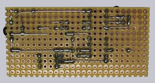
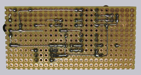
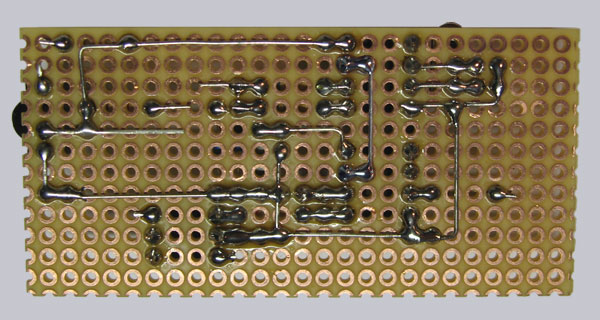
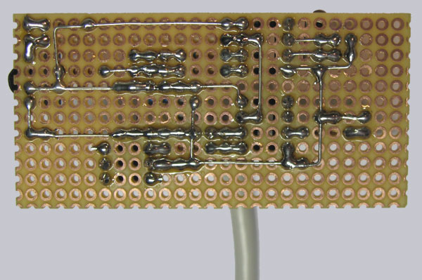
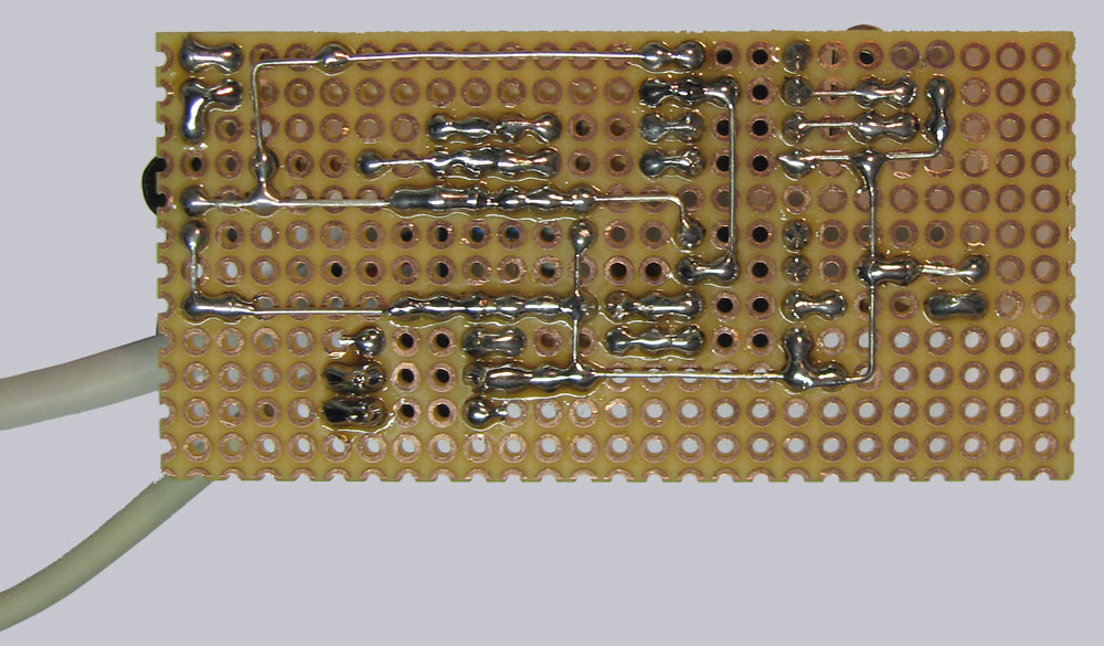
Here is a picture of the soldered lower surface …
Insert both ICs in the right direction …
Now insert the ICs with the IC notch (or the point) to the IC Socket notch (in the following picture to the right), whereby the ATTiny45-20 is alongside the quartz and the ATtiny13V-10PU is next to the Jumper. Afterwards we can put on the Jumper for the first programming …
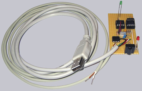
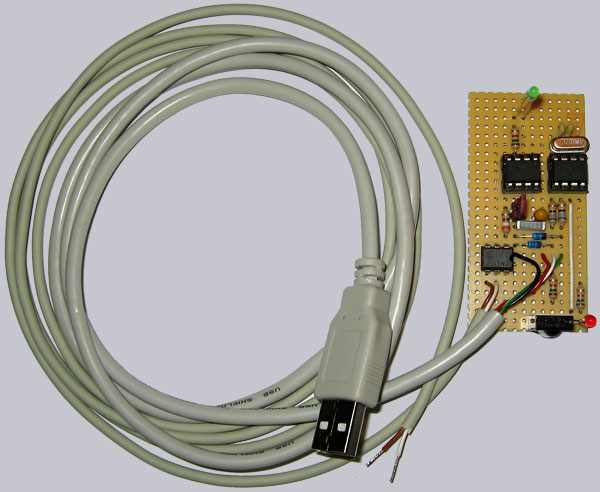
That’s it, we’ve build USB Ultra IR-receiver 2.0 … 🙂
Now control again all soldered connections and again the correct polarity. It is now rather late to discover failures, but better late than never and one can never control often enough. The power supply unit and the USB port is secured, but it’s really important to prevent all failures. Of course I’m not responsible for any damages. But if you’ve problems with late noticed solder failures, I’ll give my best to help you by E-Mail.